-
1371 Old Oakland Rd. San Jose,
CA, 95112 -
(408) 943-8760sales@networkpcb.com


Our Printed Circuit Board Fabrication abilities include a wide diversity of Densities, Layer Counts, Materials, Processes and Finishes. We are renowned for the quick turnarounds – 2 Layer PCB projects as fast as the same day or Multi-Layer PCB projects as fast as 24 hours.
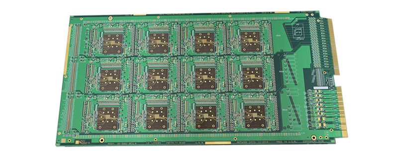
We are market leaders in the design and manufacture of Burn-in Boards (BIB). Burn in Board is a printed circuit board that functions as a jig in the Burn-in process. The Burn-in Board is used as part of the ASIC reliability testing process during which the printed circuit board components are stressed to detect failures. Burn in Boards consist of sockets to accommodate the tested ASICs and are designed to withstand high temperatures during tests. Our experts ensure that all active/passive components and connectors comply with the high-temperature requirements, and all materials and components meet the high-temperature and the oven ageing requirements.
Starting from material selection to component selection, based on the test nature, we carefully choose everything to meet the required specifications. We provide boards for all system types, with solutions available for various test conditions including HTOL, LTOL, PTC, HAST and 85/85. Each burn-in board is designed by engineers specializing in burn-in board design and can be tailored to meet the customer’s application requirements and specifications.
We provide quick turnaround time for both Universal board designs and Custom printed circuit board designs. Skilled in managing all sizes, versatile complexities, BGA, LGA, QFP, DIP, custom-sockets and multiple layers for both prototype and production quantity.
We do burn-in board manufacturing for various peak temperature ranges from 125 Deg C to 250 Deg C using High Tg FR4 or Special Polyimide materials based on the applicable test temperatures.
| Parameter | Units | |
|---|---|---|
| mm | inches | |
| Layer Count | 02 to 14 | 0.078 to 0.55 |
| Base Materials | FR-4 High Tg, Polyimide, Nelco |
FR-4 High Tg, Polyimide, Nelco |
| Thickness Range | 1.57 | 0.062" |
| 2.36 | 0.093" | |
| 3.2 | 0.125" | |
| Conductor Width | 0.08 | 0.003" |
| Conductor Space | 0.08 | 0.003" |
| Hole Diameter | ø 0.15 | ø 0.006 |
| Surface Treatment (Hard Gold & Electroless Gold Plating) |
1.3 μm | 50 μm |
| Etc | HPL | |