- 1371 Old Oakland Rd. San Jose,
CA, 95112 -
(408) 943-8760sales@networkpcb.com


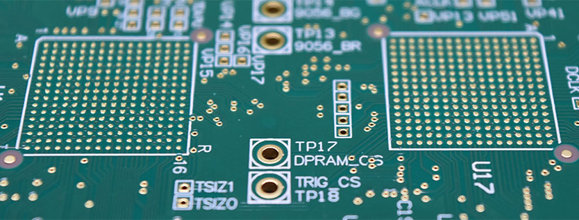
We offer High-Density Interconnect (HDI) printed circuit boards with a higher wiring density per unit area than a conventional PCB. They have much finer lines and spaces, smaller vias and capture pads, and higher connection pad density than employed in conventional PCB technology. Our HDI PCBs are made through Microvia, buried vias and sequential lamination with insulation materials and also employ conductor wiring for a higher density of routing.
Our HDI PCB with a reduced footprint, enhance the electrical performance of the application device. HDI PCB is the best alternative to high layer-count and expensive standard laminate or sequentially laminated boards. Our expertise in incorporating blind and buried vias help to save PCB real estate by allowing features and lines to be designed above or below them without making a connection. Multiple via processes, including via in pad and blind via technology, allow designers more PCB real estate to place components. Decreased PCB component size and pitch allow for more I/O in smaller geometries. This means the faster transmission of signals and a significant reduction in signal loss and crossing delays.
| Property | Typical Value | Advanced Production |
|---|---|---|
| Layer Count | 4 - 16 Layers | 4 - 20 Layers |
| PCB Thickness | 0.6 - 1.0 mm | 0.6 - 3.0 mm |
| Build up Technology | i+N+i (i≥2) HDI PCB | Any Layer Microvias Copper filled |
| Min. Laser Drill Diameter | 4 mil | 3 mil |
| Laser Technology | CO2 laser Drilling | CO2 laser Drilling |
| Materials | FR4 | FR4(HF) |
| Glass Transition(TG) | 140°C / 150°C / 170°C | 140°C / 150°C / 170°C |
| Copper Plating Holes | 12 µm / 18 µm | 12 µm / 18 µm |
| Inner Layer Registration | +/-3 mil | +/-2 mil |
| Min. Line / Spacing | 3 / 3 mil | 2.5 / 2.5 mil (BGA area) |
| Min. Annular Ring | 2.5 mil | 2.5 mil |
| Smallest Drill | 0.20 mm | 0.15 mm |