
-
1371 Old Oakland Rd. San Jose,
CA, 95112 -
(408) 943-8760sales@networkpcb.com
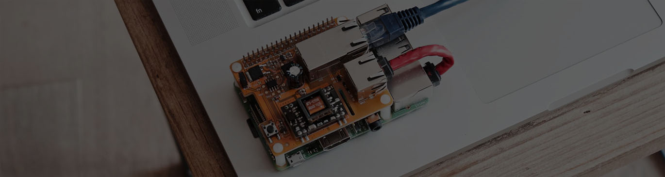
The production of Printed Circuit Boards is carried out according to the relevant IPC guidelines and standards and also according to customer defined specifications & requirements. Additionally we have the capability to produce boards of various types with tighter tolerances & also any other speciality requirements. Discuss with us for your requirements.
| Descriptional Images | Specification | Standard Design | Intermediate Design | Significant Design |
|---|---|---|---|---|
|
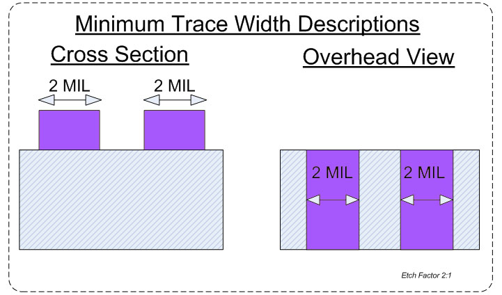
Minimum Trace Width | 0.005" | 0.003" | 0.002" |
|
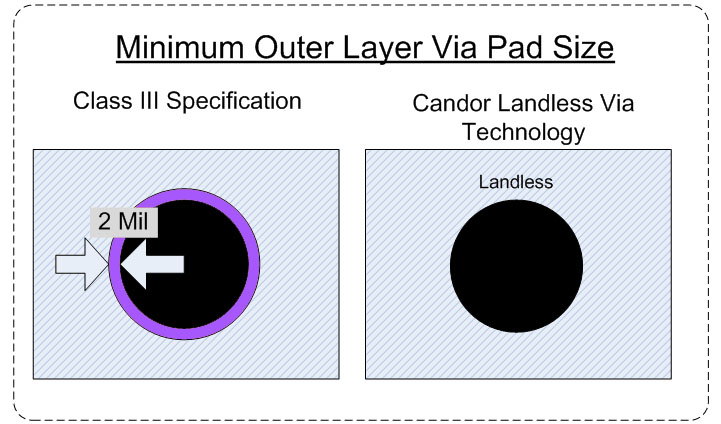
Outer Layer Via Pad Size | Class 3: 2 Mil, and capable up to landless via | 0.005" | 0.003" |
|
|
Line to Line Spacing | 0.005" / 0.005" | 0.003" / 0.003" | 0.002" / 0.002" |
|
Minimum Through Hole Drilled | 0.008" | 0.006" | 0.004" |
|
Minimum Buried Via Drilled | 0.008" | 0.006" | 0.004" |
|
|
Minimum Blind Via Drilled | 0.008" | 0.006" | 0.004" |
|
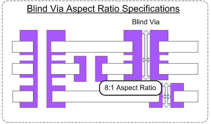
Blind Via Aspect Ratio | 8:1 Aspect Ratio | 1:1 | 1:1 |
|
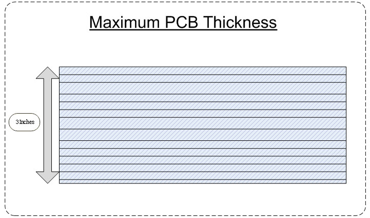
Maximum PCB Thickness | 300 mil | 0.008-0.125" | 0.002"-0.4" |
|
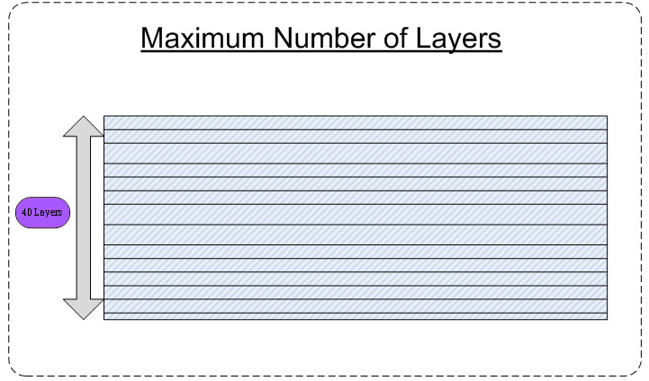
Number of Layers | 12 Layers | 22 layers | 40 layers |
|
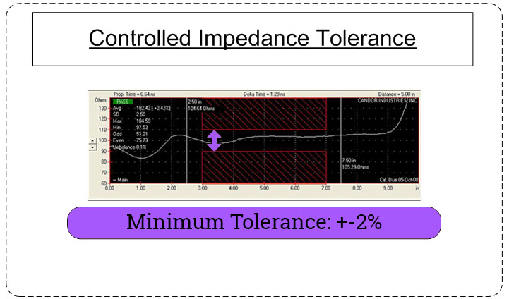
Controlled Impedance Tolerance | +- 5% or Under Tolerance | -0.05 | -0.025 |
|
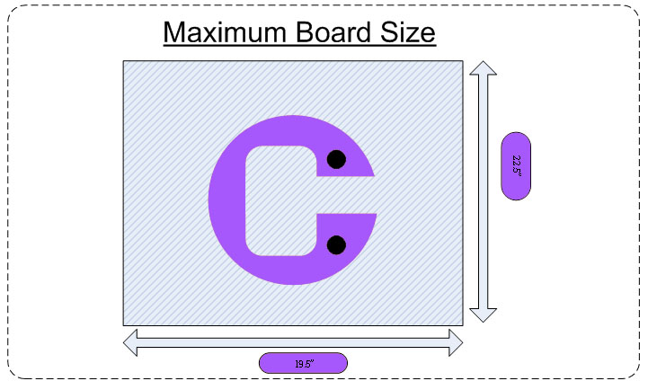
Maximum Board Size | 19.5" X 22.5" | 20.5 X 24.5" | 20.5 X 26" |
|
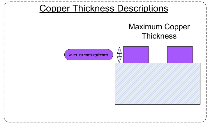
Copper Thickness/Density | Able to meet customer requirements | .25-2 oz | 5 microns-20 oz |
|
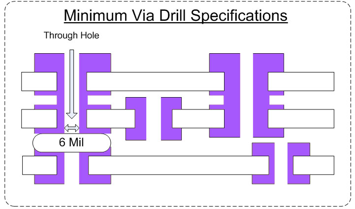
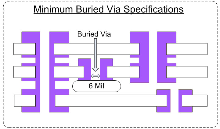
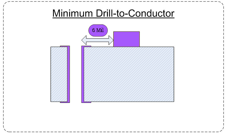
Minimum Drill-to-Conductor | 6 Mil (edge of hole to track) | 0.005" | 0.003" |
|
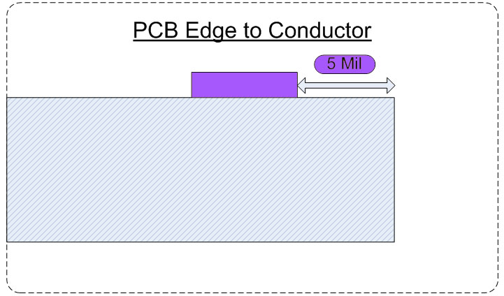
PCB Edge to Conductor | 0.010" | 0.005" | 0.002" |
|
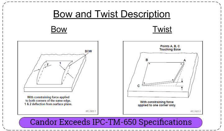
Warp (Bow and Twist) | Exceeds IPC-TM-650 | exceeds IPC Spec | exceeds IPC Spec |
|
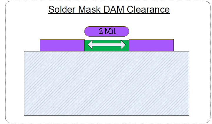
Solder Mask DAM | 0.010" | 0.005" | 0.002" |