Pioneering PCB Excellence
At Network PCB, we're more than just a PCB provider—we're pioneers in innovation. With over 3+ decades of expertise, we continually advance the limits of PCB technology, supplying forward-thinking solutions to industries across the globe.
Backed by modern facilities and a skilled engineering team, we produce high-performance, dependable PCBs for everything from everyday electronics to aerospace systems. Our unwavering focus on quality, innovation, and customer satisfaction sets us apart as a trusted partner in every project.
Our Comprehensive PCB Services
From initial design to final delivery, we provide end-to-end PCB solutions customized to your unique requirements. With deep industry expertise, we ensure every board meets the highest standards of quality, performance, and reliability—no matter the application
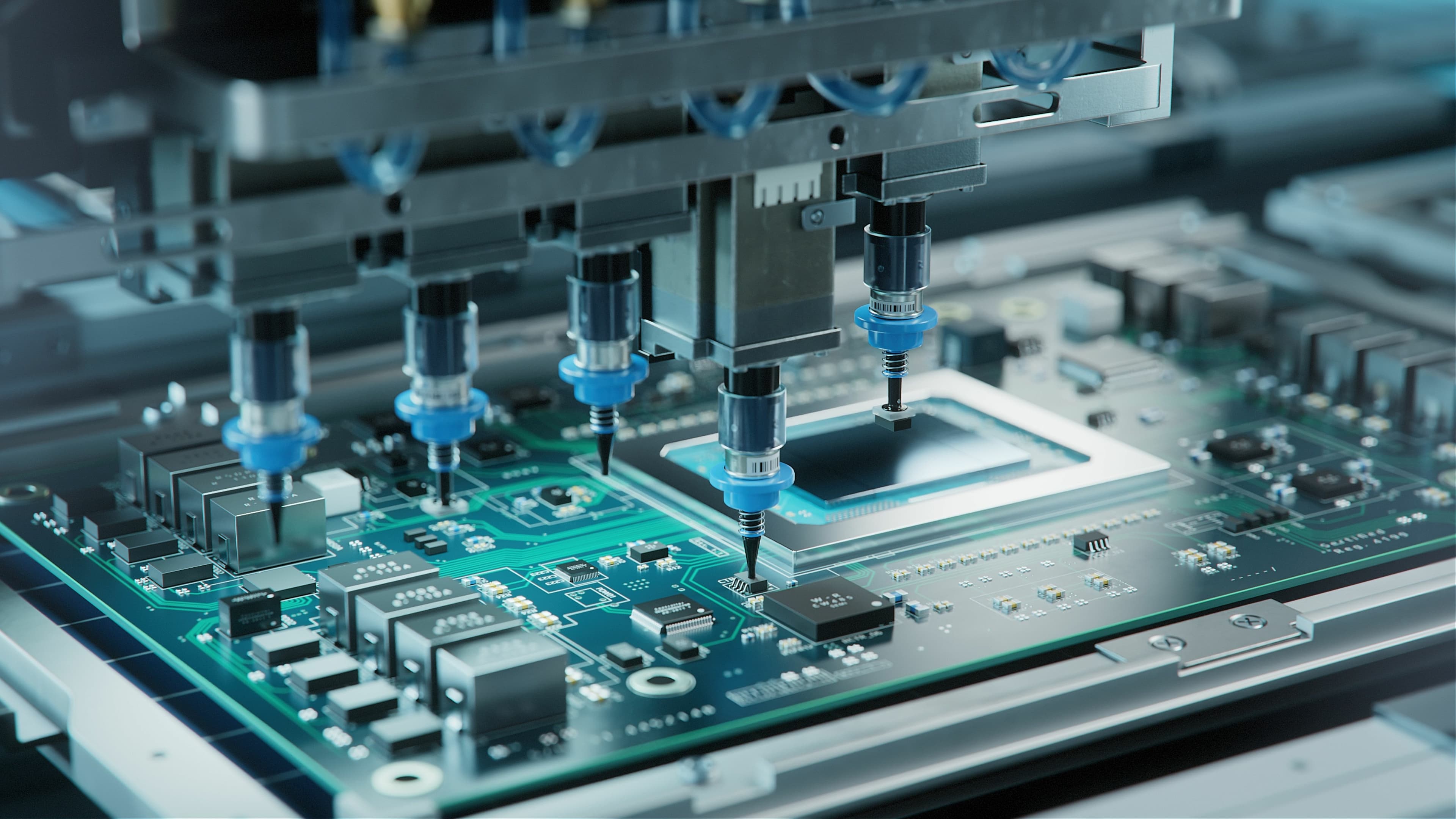
Manufacturing
Multiple Layer PCB
Complex, multi-layer PCBs for advanced applications
High Volume Production
Efficient large-scale PCB manufacturing
Prototype Fabrication
Rapid prototyping for quick iteration and testing
Assembly
PCB Assembly
Complete assembly services for your PCBs
Component Sourcing
Procurement of high-quality components
Quality Control
Rigorous testing and quality assurance
Design Support
PCB Design Review
Expert review and optimization of your designs
DFM Analysis
Design for manufacturability analysis
Technical Consultation
Expert advice on PCB design and manufacturing
Additional Services
Rush Orders
Expedited manufacturing for urgent needs
Custom Finishes
Various surface finish options available
Logistics Support
Shipping and handling of your completed PCBs
Get Your Custom PCB Quote Today
Ready to bring your PCB designs to life? Our expert team is here to provide you with a tailored quote that meets your specific requirements. Experience the Network PCB difference - where quality meets innovation.
Fast Turnaround
Get your PCBs quickly with our efficient production process
Quality Assured
We guarantee high-quality PCBs that meet industry standards
Cutting-Edge Tech
Access to the latest in PCB manufacturing technology
Custom Solutions
Tailored PCB solutions to fit your unique requirements